Designing RF PCBs for High-Frequency Applications
RF PCBs for High-Frequency Applications
High-frequency PCBs have a number of unique design considerations that must be considered in order to produce a successful circuit. These include the use of specialized materials and circuit layers, proper impedance matching, and the physical layout of components and traces. RF PCBs must also be shielded to prevent interference from external sources and other components on the board. In addition, RF PCBs must be tested and analyzed using tools such as network analyzers, spectrum analyzers, and vector signal analyzers. These tests can help identify impedance mismatches, signal reflections, and other potential problems that might affect RF performance.
In RF PCB designs, the choice of substrate material is essential to performance. Standard FR-4 boards often exhibit limitations in high-frequency applications due to their higher dielectric losses and steeper Dk versus frequency curve. Instead, a Rogers or Teflon substrate is preferred for high-performance RF applications. These specialized materials have lower loss tangents and stable dielectric constants over a range of frequencies.
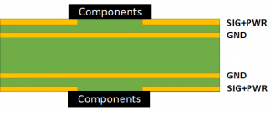
Proper impedance matching is critical for rf pcb, as even small mismatches can cause significant signal distortion and loss. To achieve good impedance, RF traces should be either microstrip or stripline geometry and have the appropriate width and spacing to match the impedance of the adjacent RF components and ground planes. Additionally, a low profile copper-dielectric interface is important for high-frequency circuits to reduce signal copper losses and ensure signal integrity.
Designing RF PCBs for High-Frequency Applications
Other factors that impact RF circuits include the routing of traces and components and the isolation of signals to prevent cross-talk between lines and unintentional antennas that can radiate or pick up other RF signals. In addition, high-frequency signals are susceptible to temperature fluctuations within the circuit. To minimize this effect, it’s important to maintain an adequate supply of decoupling capacitance between the power and ground pins. Finally, RF signal paths should be kept short and routed away from high-speed digital traces and power planes to avoid unwanted coupling and signal degradation.
Iterative testing and refinement are a critical part of RF PCB design. Testing and analysis with tools like network analyzers and spectrum analyzers can help identify areas where improvements can be made, such as reducing signal loss or preventing cross-talk between components. These findings can then be used to make design changes that improve the quality of the RF circuit.
RF PCB design is an intricate process that requires a thorough understanding of the principles of physics and electrical engineering. By following a comprehensive RF design process and applying the best practices, designers can create reliable and high-performance RF circuits. By collaborating closely with the manufacturing team, designers can ensure that the RF PCBs produced meet the required specifications. This includes performing post-manufacturing testing and analysis with tools such as time-domain reflectometry to identify any impedance mismatches, signal reflectivity, and other defects that may adversely affect RF performance. In addition, electromagnetic simulation software can be used to optimize RF designs and provide accurate prediction of circuit performance.